VHDL coding tips and tricks: April 2010

Monday, April 26, 2010

How to implement State machines in VHDL?

    A finite state machine (FSM) or simply a state machine, is a model of behavior composed of a finite number of states, transitions between those states, and actions.It is like a "flow graph" where we can see how the logic runs when certain conditions are met.
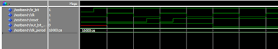
    In this aricle I have implemented a Mealy type state machine in VHDL.The state machine bubble diagram in the below figure shows the operation of a four-state machine that reacts to a single input "input" as well as previous-state conditions.
The code is given below:

library ieee;
use IEEE.std_logic_1164.all;

entity mealy is
port (clk : in std_logic;
      reset : in std_logic;
      input : in std_logic;
      output : out std_logic
  );
end mealy;

architecture behavioral of mealy is

type state_type is (s0,s1,s2,s3);  --type of state machine.
signal current_s,next_s: state_type;  --current and next state declaration.

begin

process (clk,reset)
begin
 if (reset='1') then
  current_s <= s0;  --default state on reset.
elsif (rising_edge(clk)) then
  current_s <= next_s;   --state change.
end if;
end process;

--state machine process.
process (current_s,input)
begin
  case current_s is
     when s0 =>        --when current state is "s0"
     if(input ='0') then
      output <= '0';
      next_s <= s1;
    else
      output <= '1';
      next_s <= s2;
     end if;  

     when s1 =>        --when current state is "s1"
    if(input ='0') then
      output <= '0';
      next_s <s3;
    else
      output <= '0';
      next_s <= s1;
    end if;

    when s2 =>       --when current state is "s2"
    if(input ='0') then
      output <= '1';
      next_s <= s2;
    else
      output <= '0';
      next_s <= s3;
    end if;


  when s3 =>         --when current state is "s3"
    if(input ='0') then
      output <= '1';
      next_s <= s3;
    else
      output <'1';
      next_s <= s0;
    end if;
  end case;
end process;

end behavioral;

I think the code is self explanatory.Depending upon the input and current state the next state is changed.And at the rising edge of the clock, current state is made equal to next state.A "case" statement is used for jumping between states.
The code was synthesised using Xilinx XST and the results are shown below:

---------------------------------------------------------

States                      4                                            
Transitions                 8                                            
Inputs                      1                                            
Outputs                     4                                            
Clock                       clk (rising_edge)                  
Reset                       reset (positive)                
Reset type                  asynchronous                          
Reset State                 s0                        
Power Up State              s0                              
Encoding                    Automatic                        
Implementation              LUT

---------------------------------------------------------

Optimizing FSM on signal with Automatic encoding.
-------------------
 State | Encoding
-------------------
 s0    | 00
 s1    | 01
 s2    | 11
 s3    | 10
-------------------

   Minimum period: 0.926ns (Maximum Frequency: 1080.030MHz)
   Minimum input arrival time before clock: 1.337ns
   Maximum output required time after clock: 3.305ns
   Maximum combinational path delay: 3.716ns

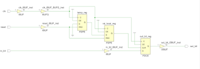
The technology schematic is shown below:

     As you can see from the schematic, XST has used two flipflops for implementing the state machine.The design can be implemented in hardware using many FSM encoding algorithms.The algorithm used here is "Auto" which selects the needed optimization algorithms during the synthesis process.Similarly there are other algorithms like one-hot,compact,gray,sequential,Johnson,speed1 etc.The required algorithm can be selected by going to Process -> Properties -> HDL options -> FSM encoding algorithm in the main menu.Now select the required one, from the drop down list.
More information about these options can be found here.

A very popular encoding method for FSM is One-Hot, where only one state variable bit is set, or "hot," for each state.The synthesis details for the above state machine implementation using One-hot method is given below:

Optimizing FSM on signal with one-hot encoding.
-------------------
 State | Encoding
-------------------
 s0    | 0001
 s1    | 0010
 s2    | 0100
 s3    | 1000
-------------------

   Minimum period: 1.035ns (Maximum Frequency: 966.464MHz)
   Minimum input arrival time before clock: 1.407ns
   Maximum output required time after clock: 3.418ns
   Maximum combinational path delay: 3.786ns

The Technology schematic is shown below:
    The main disadvantage of One-hot encoding method can be seen from the schematic.It uses 4 flip flops while, binary coding which is explained in the beginning of this article, uses only 2 flip flops.In general, for implementing a (2^n) state machine , binary method take n-flip flops while one hot method takes (2^n) flip flops.
But there are some advantages with one-hot method:
1)Because only two bits change per transition, power consumption is small.
2)They are easy to implement in schematics.

Monday, April 19, 2010

VHDL: 8 bit Binary to BCD converter with Testbench

    All numerical values are fundamentally handled as binary numbers inside the FPGA. But that is not so human readable, isnt it? Even when we write a VHDL program, most of us would prefer to write, 
a <= 10; instead of a <= "1010";.

    When viewing signals in a simulation waveform, we can easily change the radix of the signal as per our convenience. But when we test the design on a real FPGA board, we would need to use dedicated display panels such as 7 segment decoders to see the binary numbers in decimal format. This is where BCD format comes in. 

    The decimal number 10, when converter to BCD format would be "10". Looks the same, except that, here each digit is given 4 bits for their storage. Though 4 bits can store from 0 to 15, we limit the range from 0 to 9, just like that of a regular decimal number.

    In this blog post, I want to share a VHDL function for converting an 8 bit binary number into a 3 digit (or 12 bit binary) BCD number. BCD stands for Binary Coded Decimal. The algorithm used is known as double dabble. You can read more on it here at, Double Dabble(wiki).

    A self checking testbench has been written as well, to verify the function. 

BCD Converter + Testbench:


library ieee;
use ieee.std_logic_1164.all;
use ieee.numeric_std.all;

--empty entity for testbenches.
entity tb_bcd_conversion is
end tb_bcd_conversion;

architecture Behavioral of tb_bcd_conversion is

--Function definition
function to_bcd ( bin : unsigned(7 downto 0) ) return unsigned is
    variable i : integer:=0;
    variable bcd : unsigned(11 downto 0) := (others => '0');
begin
    for i in 7 downto 1 loop  --iterating 7 times.
        --left shifting the bits and padding to the lsb
        bcd := bcd(10 downto 0) & bin(i);  
        --increment 3 if BCD digit at 1's is greater than 4.
        if(bcd(3 downto 0) > 4) then 
            bcd(3 downto 0) := bcd(3 downto 0) + 3;
        end if;
        --increment 3 if BCD digit at 10's is greater than 4.
        if(bcd(7 downto 4) > 4) then 
            bcd(7 downto 4) := bcd(7 downto 4) + 3;
        end if;
        --we dont need to repeat the above if statement for 100's position. Why?
        --Because input is 8 bit, which means maximum value at 100's position is 2.
    end loop;
    bcd := bcd(10 downto 0) & bin(0);  --final left shifting
    return bcd;  --return the result
end function to_bcd;
--End of function definition

--signals used to test the function.
--They help us to view the results in simulation waveform
signal bcd_out : unsigned(11 downto 0);
signal bcd_out_int: integer;

begin

--process where we test the binary to bcd function
stimulus_process: process
--variables used for testing. 
--Varibales are useful because they get updated rightaway.
--But they cant be seen in simulation waveform, thats why we assign
--them to signals before exiting the process.
variable bcd_out_int_var : integer;
variable bcd_out_var : unsigned(11 downto 0);
begin
    --test for all the 256 values the 8 bit input can take.
    for i in 0 to 255 loop
        bcd_out_var := to_bcd(to_unsigned(i,8));
        --convert bcd to decimal value by multiplying respective digits with 1,10 and 100.
        bcd_out_int_var := to_integer(bcd_out_var(3 downto 0)) + 
            to_integer(bcd_out_var(7 downto 4))*10 +  
            to_integer(bcd_out_var(11 downto 8))*100;
        --the assert statement is used to implement a self checking testbench.
        --we dont need to manually verify if each input is correctly converted,
        --but the testbench does it for us. If the statement in the 'assert' is
        --incorrect a 'warning' message will be reported in modelsim
        assert bcd_out_int_var = i;
        --assign to signals to see the results in simulation waveform
        bcd_out_int <= bcd_out_int_var;
        bcd_out <= bcd_out_var;
        --let the results stay the same for some time, so that human eyes could catch it.
        wait for 10 ns;
    end loop; 
    wait;  --testing done. wait Endlessly.
end process;

end Behavioral;


Simulation Waveform:


Some sample inputs and the corresponding outputs are shown below:
binary = "01100011",      output = "0000 1001 1001"  (99).
binary = "11111110",      output = "0010 0101 0100"  (254).
binary = "10111011",      output = "0001 1000 0111"  (187).

A part of the simulation waveform from Modelsim is shared below:


simulation waveform of binary to bcd converter in vhdl modelsim


Schematic after synthesis:


The code was synthesised using Xilinx Vivado 2023.2. The schematic generated after synthesis is shared below:

schematic from xillinx vivado for bcd converter


Note :- The code can be modified to convert any length binary number to corresponding BCD digits. This require very little change in the code. May be you could try that as a homework. 

Wednesday, April 14, 2010

VLSI Interview Questions - Part 2

This is part-2 of the interview questions series. Hope it is useful.

1)For the circuit shown below, what should the function F be, so that it produces an output of the same frequency (function F1), and an output of double the frequency (function F2).

a. F1= NOR gate and F2= OR gate
b. F1=NAND gate and F2= AND gate
c. F1=AND gate and F2=XOR gate
d. None of the above


Ans : (c) . (Hint : Assume a small delta delay in the NOT gate).

2)The maximum number of minterms realizable with two inputs (A,B) is:

Ans : For n bits the max number minterms is, (2^n).
For n=2, no. of minterms = (2^2) =  4.
http://www.iberchip.net/VII/cdnav/pdf/75.pdf

3)The maximum number of boolean expressions with two inputs (A,B) is:

Ans : For n bits the max number boolean expressions are, 2^(2^n).
For n=2, no. of boolean expressions = 2^(2^2) =  2^4 = 16.
http://www.iberchip.net/VII/cdnav/pdf/75.pdf

4) A ring counter that counts from 63 to 0 will have ______ D flip-flops,
but a binary counter that counts from 63 to 0 will have _____ D flip-flops

Ans : For ring counter 64. for binary counter 6.

5) Why cache memory is used in computers?

    Cache memory is used to increase the speed of memory access by processor. Unlike the main(physical) memory cache memory is small and has very short access time. The most recent data accessed by processor is stored in cache memory. This will help the processor to save time because time is not wasted in accessing the same data from the main memory again and again.

    A good example is that, if processor is executing a loop 1000 times involving many variables(so that the CPU registers available are all used up) then the value of these variables can be stored in cache memory. This will make the loop execution faster.

    In designing cache, cache miss probability and hit probability determines the efficiency of the cache and the extend to which the average memory access time can be reduced.

6) How will you design a sequence detector?

See this link:
http://web.cs.mun.ca/~paul/cs3724/material/web/notes/node23.html

7) What is setup time and holdtime?

    Setup time is the minimum amount of time before the clock’s active edge by which the data must be stable for it to be detected correctly. Any violation in this will cause incorrect data to be captured.
(Analogy for setup time: Suppose you have to catch a train and the train leaves at 8:00. Say you live 20 minutes away from the station, when should you leave your house?
Ans : at 7:40 -> set up time is 20 mins in this case)

    Hold time is the minimum amount of time after the clock’s active edge during which the data must be stable. Any violation in this required time causes incorrect data to be latched.
(Suppose your friend needs help in boarding the train and train only allows 5 mins for boarding. How long should you stay after you have arrived?
Ans : Atleast 5 mins -> Hold time is 5 mins )
A very good tutorial with examples about setup time and hold time can be found at this link:
http://nigamanth.net/vlsi/2007/09/13/setup-and-hold-times/

8)What is the difference between Moore and Mealy state machines?

Ans : Moore and Mealy state machines are two ways of designing a state machine. 

    Moore state machines are controlled in such a way that the outputs are a function of the current state alone. Mealy state machines are controlled in such a way that the outputs depend on the current state and the current inputs. 

    A Moore state machine may require more states(but less complex) than a Mealy state machine to accomplish the same task.

VLSI Interview Questions - Part 1

     Here are some common interview questions asked by some VLSI companies. Try to learn the concept used in solving the questions rather than blindly going through the answers. If you have any doubts drop me a note in the comment section.

1) Design a full adder using halfadders.

Ans :
full adder using halfadders

2) Find the value of A,B,C in the following circuit, after 3 clock cycles.  (ST Microelectronics)


This is a simple Ring counter. An n-bit ring counter has n states. The 3-bit counter shown above has 3 states and they are : 100 , 010 , 001 , 100 and so on..
So after 3 clock cycles  A,B,C = 100.

3) Design XOR gate using 2:1 MUX.    (Intel)

Ans :       

4) If A=10 and B=20, without using temporary register how can you interchange the two things?   (Intel) 

Ans :
    Perform the following operations sequentially:
         A = A xor B;
         B = A xor B;
         A = A xor B;
  Now A=20 and B=10.

5)What is the expression for 
output 'y' in the following circuit?

Ans : (In the notation I have used, A' means not(A), and AB means (A and B).
y = ( A'B'C + AB'C' + A'BC + ABC' )
  = ( A'C (B+B') + AC' (B+B') )
  = A'C + AC'
  = A xor C.

6)The input combination to find the stuck at '0' fault in the following circuit is:  (Texas Instruments)


Ans : X is always zero in the above circuit. So P is always zero whatever the value of A,B,C or D is.
To check the fault at X, make either inputs C or D zero, and A,B as '1'. So the input combination is "1101".

7)Consider a two-level memory hierarchy system M1 & M2. M1 is accessed first and on miss M2 is accessed. The access of M1 is 2 nanoseconds and the miss penalty (the time to get the data from M2 in case of a miss) is 100 nanoseconds. The probability that a valid data is found in M1 is 0.97. The average memory access time is:

Ans : This question is based on cache miss and success probability.
Average memory access time = (Time_m1 * success_prob ) + ( (Time_m1 + Time_m2) * miss_prob)
                    = ( 2* 0.97 ) + ( (2+100) * (1- 0.97) )
                    =  1.94 + 3.06 = 5 ns.

8)Interrupt latency is the time elapsed between:
a. Occurrence of an interrupt and its detection by the CPU
b. Assertion of an interrupt and the start of the associated ISR
c. Assertion of an interrupt and the completion of the associated ISR
d. Start and completion of associated ISR.

Ans : (b). ISR means Interrupt service routine.

These are only some of the questions I have seen. More questions will be up soon. 

Tuesday, April 13, 2010

VHDL: Synchronous Vs Asynchronous Resets

    A reset is used to initialize the signals in your design to a predetermined state. Broadly speaking, there are two ways in which we can apply a reset signal in VHDL: Synchronous or asynchronous

    The next question you would probably ask is, so which one should I choose? Which is the best? Unfortunately the answer isnt that simple. It depends on many factors and even among experts there is no consensus on this matter. So, we wont try to answer this question here. But what I would try, is to give a general idea on the various types of reset which will help you make the best decision suitable for your project.

1. Purely Synchronous Reset:


A synchronous reset signal can be coded in VHDL as shown below :

library ieee;
use ieee.std_logic_1164.all;

entity sync_reset is
port(clk : in std_logic;  --clock
    reset : in std_logic; --active high reset
    in_bit : in std_logic;
    out_bit_sync : out std_logic
);
end sync_reset;

architecture Behavioral of sync_reset is

begin

process(clk)
begin
    if(rising_edge(clk)) then
        if(reset = '1') then  --reset is checked only at the rising edge of clock.
            out_bit_sync <= '0';
        else
            out_bit_sync <= in_bit;
        end if;
    end if;
end process;

end Behavioral;

You can see that the value of reset input is only checked at the rising edge of the clock signal. That is why it is called a synchronous reset. Look at the below simulation waveform from Modelsim to get a better understanding of the code.

synchronous reset, simulation waveform in modelsim vhdl

    The in_bit is sampled only at the rising edge of the clock cycle. The short reset pulse is ignored because it didnt align with any of the rising edges of the clock. The reset signal was asserted again, but it wasnt sampled until the next rising edge of the clock, upon which the output bit was set to '0'.

When synthesised, Xilinx Vivado tool generated the following schematic for the above code:

synchronous reset. fdre in xilinx vivado schematic

    Ignoring the buffers for inputs and output, the tool uses a single flipflop, FDRE for implementing this code. Xilinx doc on FDRE says:
FDRE is a single D-type flip-flop with data (D), clock enable (CE), and synchronous reset (R) inputs and data output (Q). The synchronous reset (R) input, when High, overrides all other inputs and resets the (Q) output Low on the Low-to-High clock (C) transition. The data on the (D) input is loaded into the flip-flop when R is Low and CE is High during the Low-to-High clock transition.

Now, lets look into the pros and cons of this(synchronous reset) approach.

Pros

  1. The reset applied to all the flip-flops are fully synchronized with clock and always meet the reset recovery time. Reset recovery time is the minimum time between the de-assertion of a reset and the clock signal being high again. 
  2. In some cases, synchronous resets will reduce the number of flipflops used at the expense of combinational logic gates. So this may not be truly an advantageous point.

Cons

  1. If the reset pulse is not wide enough then the clock edge may not be able to capture the reset signal. Thus, if you use synchronous resets make sure that your reset signal stays active for enough time so that it gets captured by the clock.
  2. The change in reset input doesn't immediately reflect in the signals which are to be reset.
  3. Synchronous resets have high fan-outs. Fan-out refers to the maximum number of output signals that are fed by the output equations of a logic cell. High fan-out makes it difficult to meet timing constraints without pipelining and duplicating the synchronous reset source
  4. Synchronous resets, by their very nature, needs a clock in order to work. This can be annoying, for example, if you are using a gated clock. As the reset will go unregistered if the reset is asserted, when the clock is disabled to save power.

2. Purely Asynchronous Reset:


An asynchronous reset signal can be coded in VHDL as shown below :

library ieee;
use ieee.std_logic_1164.all;

entity async_reset is
port(clk : in std_logic;  --clock
    reset : in std_logic; --active high reset
    in_bit : in std_logic;
    out_bit_async : out std_logic
);
end async_reset;

architecture Behavioral of async_reset is

begin

process(clk,reset)
begin
    if(reset = '1') then  --change in reset get immediately reflected on output
        out_bit_async <= '0';
    elsif(rising_edge(clk)) then
        out_bit_async <= in_bit;
    end if;
end process;

end Behavioral;

You can see that the value of reset input is checked irrespective of any event from the clock signal. That is why this is called a asynchronous reset. Look at the below simulation waveform from Modelsim to get a better understanding of the code.

asynchronous reset in vhdl. simulation waveform in modelsim,


You can see that, contrary to the first simulation, the reset takes effect immediately and sets the output bit to '0'.

When synthesised, Xilinx Vivado tool generated the following schematic for the above code:

Asynchronous reset. fdce in xilinx vivado schematic

     Ignoring the buffers for inputs and output, the tool uses a single flipflop, FDCE for implementing this code. Xilinx doc on FDCE says:

FDCE is a single D-type flip-flop with clock enable and asynchronous clear.

  • When clock enable (CE) is High and asynchronous clear (CLR) is Low, the data on the data input (D) of this design element is transferred to the corresponding data output (Q) during the Low-to-High clock (C) transition.
  • When CLR is High, it overrides all other inputs and resets the data output (Q) Low.
  • When CE is Low, clock transitions are ignored.

Now, lets look into the pros and cons of this(Asynchronous reset) approach.

Pros

  1. Signals can be reset without waiting for the clock edge to arrive. Or in general, the clock needn't even be there.
  2. If the FPGA vendor library has asynchronously resettable flip flops then the data path will be clean. This is because there is no need to place any extra logic gates on the data-path to implement the reset.

Cons

  1. If the asynchronous reset is released at or near the active clock edge of a flip-flop, the output of the flip-flop could go metastable and thus the reset state could be lost. This is not so much of a dangerous issue on assertion of reset, but could be disastrous at de-assertion. 
  2. Depending on the source, sometimes resets may occur spuriously due to noise or glitches on the board or system reset. All such events will be counted as valid resets.

3. Asynchronous Assertion, Synchronous De-assertion:


    So we see that, both synchronous and asynchronous resets have their pros and cons. Is there a way to get the best of both in some way? Yes, and that is where this third approach comes in. 

    We can assert the reset synchronously and de-assert it asynchronously. Such a circuit is called a reset synchronizer. Let us see how this can be done in VHDL: 

library ieee;
use ieee.std_logic_1164.all;

entity reset_synchronizer is
port(clk : in std_logic;  --clock
    reset : in std_logic; --active high reset
    in_bit : in std_logic;
    out_bit : out std_logic
);
end reset_synchronizer;

architecture Behavioral of reset_synchronizer is

signal rst_local, temp : std_logic;

begin

--create a local reset from reset input
process(clk,reset) begin if(reset = '1') then --assert reset asynchronously temp <= '1'; rst_local <= '1'; elsif(rising_edge(clk)) then --deassert reset synchronously temp <= '0'; rst_local <= temp; end if; end process;
--use the local reset generated to manipulate the main logic
process(clk,rst_local) begin if(rst_local = '1') then --local reset is used to reset the output out_bit <= '0'; elsif(rising_edge(clk)) then out_bit <= in_bit; end if; end process; end Behavioral;

    We use two processes to implement this circuit. First process generates a local reset signal called rst_local and the second process uses the generated local reset and clock to implement the desired logic. 

    When the reset is just asserted, the local reset immediately follows it, but when its de-asserted, it has to travel through two D flipflops to be reflected in the local reset. What is the use of this? This means that, the reset we use locally, stays for one whole clock cycle before its de-asserted and it wont de-assert just before a clock's positive edge. This resolves a major disadvantage of asynchronous resets.

    Look at the below simulation waveform from Modelsim to get a better understanding of the code. You can see that how the output bit changes right away when the reset is asserted, but takes at least one clock cycle to change when its de-asserted.

reset synchronizer in vhdl. simulation waveform from modelsim


When synthesised, Xilinx Vivado tool generated the following schematic for the above code:

schematic of reset synchronizer in xilinx vivado

     Ignoring the buffers for inputs and output, the tool uses 3 flipflops - two FDPE's(used for generating the local reset) and one FDCE(used for the main logic). 

    If you scroll up you can see that FDCE was used for implementing asynchronous reset. FDCE has an asynchronous clear input. This clear input is driven from the Q output of the second FDPE flip flop. 

    What is FDPE? It is a single D-type flip-flop with data (D), clock enable (CE), and asynchronous preset (PRE) inputs and data output (Q). The asynchronous PRE, when High, overrides all other inputs and sets the (Q) output High. The PRE input of FDPE flipflop is connected to the reset input to the design. First flip flop's D input is connected to '0' and its Q is connected to D of the second flipflop. This makes the reset travel through the flipflops when its de-asserted.

Now, lets look into the pros and cons of this approach.

Pros

  1. The circuit doesn't have metastability problems.
  2. The circuit can be reset right away, without waiting for the clock edge to arrive.

Cons

  1. Once the reset is de-asserted, it still takes a minimum of one clock cycle for the system to come out of reset-state.
  2. Depending on the source, sometimes resets may occur spuriously due to noise or glitches on the board or system reset. All such events will be counted as valid resets.
  3. Similar to synchronous resets, this type of resets wont always work with gated clocks. The reset will go unregistered, if the reset is asserted when the clock is disabled to save power.


References:-


Conclusion:-


As stated in the beginning of this post, there is no single approach that works best for all scenarios when it comes to resets. Lay down the characteristics of your system, look into what resources are available in the FPGA you are targeting and then decide what suits your design best.

Happy resetting! :)

VHDL: Does Process Sensitivity List Matter In Simulation or Synthesis?

    You might have encountered this error while trying to synthesis your VHDL code: One or more signals are missing in the process sensitivity list (or)  signal 'xxx' is read in the process but is not in the sensitivity list. In this article I want explain if there is any relation between the process sensitivity list and synthesis results.

Let us look at an example:

library ieee;
use ieee.std_logic_1164.all;

entity test1 is
port(clk : in std_logic;
    rst : in std_logic;
    a,b : in std_logic;
    c,d : out std_logic
);
end test1;

architecture Behavioral of test1 is

begin

--Synchronous process(some flipflop's are used for implementation)
process(clk,rst)
begin
    if(rst = '1') then
        c <= '0';
    elsif(rising_edge(clk)) then
        c <= a;
    end if;
end process;

--combinational process(some LUT's are used for implementation)
process(a,b)
begin
    d <= a and b;
end process;

end Behavioral;

The code has one synchronous process, which assigns the input a to output c. It also has a combinatorial process which does an and operation on inputs a and b and assigns the result to d.

The following testbench code was used for testing the functionality of the above code:

library ieee;
use ieee.std_logic_1164.all;

entity testbench is
end testbench;

architecture Behavioral of testbench is
    --inputs
    signal a,b : std_logic := '0';
    signal clk : std_logic := '0';
    signal rst : std_logic := '0';
        --outputs
    signal c,d : std_logic := '0';
    -- clock period definitions
    constant clk_period : time := 10 ns;
begin

    -- instantiate the unit under test (uut)
    uut: entity work.test1 port map (
        clk => clk,
        rst => rst,
        a => a,
        b => b,
        c => c,
        d => d);

   -- clock process definitions
    clk_process :process
    begin
        wait for clk_period/2;
        clk <= not clk;  --keep toggling the clock once half of the clock period is over
    end process;

    -- stimulus process
    stim_proc: process
    begin  
        a <= '1';   b <= '1';     
        wait for clk_period;
        --try reset
        wait for clk_period/4;
        rst<='1';
        wait for clk_period;
        rst<='0';
        b <= '0';
        wait;
    end process;

end;

The simulation waveform is shared few scrolls down and verifies that the code is working as its supposed to. 

Let's also synthesis the code. I used Xilinx Vivado 2023.2 for this. The schematic generated by Vivado is shared below. It confirms that the logic we wrote behavioral code for, is correctly implemented in hardware. 

schematic in xilinx vivado. sensitivity list


Now, in order to check the effect of process sensitivity on simulation or synthesis, we will make the following changes in the code:
  1. Use process(rst)  instead of process(clk,rst).
  2. Use process(b) instead of process(a,b).
Simulate the design once more using the same testbench code. Let me share both the simulation waveforms in one image, so that you can easily compare them.

simulation waveform in modelsim for process sensitivity list


    What do you notice? The simulation waveform seems to be affected by the minor changes we have made to the process sensitivity list. 
  • The change in rst doesnt cause a change in output c right away. The synchronous process, as if, waits until the change in clk happens to get activated again.
  • As for the second combinatorial process, the change in b doesnt cause any change in output d. This is because b is not in the process sensitivity list. 
So, clearly, for simulation to work well, you need to add all the read signals to the process sensitivity list. 

Now, lets synthesis the design. The synthesis is successfully  completed without any errors and it even generated the exact schematic shared previously in this article. This means that the second code will work in the same way as the first one. But I do get the following two warnings:
[Synth 8-614] signal 'rst' is read in the process but is not in the sensitivity list
[Synth 8-614] signal 'b' is read in the process but is not in the sensitivity list 

So what about the warning? After going through some online forums I found the following reasons for this warning:

  • Usually the behavior in the equations inside a process is what is intended, the sensitivity list is just a bookkeeping chore. It doesnt have anything to do with synthesis.
  • Technically what XST(Xilinx synthesis tool) have implemented is not what your VHDL code says to do as per the VHDL language definition. They are taking somewhat of a guess about what you really intended to do. By violating the language specification they implement it the way they think you 'really' want it and kick out a warning to let you know that the actual implementation will operate differently than your simulation shows.
           (Thanks KJ for your answer)

    One more thing to note is that, if the signals are synchronous(meaning inside the rising_edge(clk) statement), then they dont need to be in the sensitivity list. You might have noticed that even when the signal a is read in the first process, it wasnt included in the sensitivity list.

Conclusion :- Sensitivity list has nothing to do with synthesis. But without the proper sensitivity list, the process will not work in simulation. So as a good practice include all the signals which are read inside the process, in the sensitivity list. The results may be varied if you are using some other tool. I have used Xilinx Vivado 2023.2 version for this analysis.

Thursday, April 8, 2010

VHDL: Difference between rising_edge(clk) and (clk'event and clk='1')

    Generally you might have noticed that there are two ways in which we can detect the edge of a clock. 
  1. rising_edge(clk) or falling_edge(clk).
  2. clk'event and clk='1' or clk'event and clk='0'

    You might have been using either of these methods without really understanding if there is a difference between them. But there is a difference between them and this article intends to bring clarity on this.

Consider the following VHDL snippet:

clk_process : process
begin
    clk <= '0';
    wait for clk_period/2; --for 0.5 ns signal is '0'.
    clk <= '1';
    wait for clk_period/2; --for next 0.5 ns signal is '1'.
end process;

process(clk)
begin
    if(rising_edge(clk)) then
        xr <= not xr;
    end if;

    if(clk'event and clk='1') then
        x0 <= not x0;
    end if;
end process;

When the value of clk goes from '0' to '1', that is when it changes from low to high, I toggle the bits, xr and x0. If you run the above code, the simulation waveform will look like this:

vhdl rising edge and clk'event difference

Now you may ask where is the difference? There is no difference in this particular case. But let us slightly change the code snippet as follows:

clk_process : process
begin
    clk <= 'Z';          ----------Here is the change('Z' instead of '0').
    wait for clk_period/2; --for 0.5 ns signal is 'Z'.
    clk <= '1';
    wait for clk_period/2; --for next 0.5 ns signal is '1'.
end process;

process(clk)
begin
    if(rising_edge(clk)) then
        xr<= not xr;
    end if;

    if(clk'event and clk='1') then
        x0 <= not x0;
    end if;
end process;

The only difference in the new code is that instead of clk toggling between '0' and '1', we toggle it between 'Z' and '1'. Lets look at the simulation waveform:

vhdl rising edge and clk'event difference

Does this ring any bells? You can see that the signal xr doesn't change at all, while x0 changes just like it did in the first snippet. Why? To know why, lets look at the definition of rising_edge function as implemented in std_logic_1164 library:

FUNCTION rising_edge (SIGNAL s : std_ulogic) RETURN BOOLEAN IS
BEGIN
    RETURN (s'EVENT AND (To_X01(s) = '1') AND (To_X01(s'LAST_VALUE) = '0'));
END;

    As you can see the function returns TRUE only when the present value is '1' and the last value is '0'. If the past value is something like 'Z','U' etc. then it will return FALSE. This makes the code bug free, because the function returns only valid clock transitions, that means '0' to '1'. All the rules and examples shared above equally apply to falling_edge() function also.

The statement clk'event and clk='1' results in TRUE when the present value is '1' and there is an edge transition in the clk. It doesnt check whether the previous value is '0' or not.

Note :- Use rising_edge() or falling_edge() functions instead of clk'event statements in your VHDL projects.