VHDL coding tips and tricks: March 2010

Wednesday, March 31, 2010

VHDL: Reading and Writing Real Numbers From a File

    If you want to test your VHDL design with a large number of inputs, then its not efficient or reader-friendly to put all the inputs directly into your testbench code. One option is to store the inputs in a text file and let the testbench read the contents of it as needed. Similarly it makes sense to write the outputs of your design to a file, which can be read with another software, lets say Matlab, for verification. 

      There are lot of ways in which this can be done. Each project probably requires a different approach. In this example, I have one file 1.txt where few real real numbers are saved. The example code reads each line from the input file(1.txt), extracts the real number from the read line and writes to another file, 2.txt, in a specific format.

Let me share the VHDL code for this.

Reading and writing real numbers from a file:


--include this library for file handling in VHDL.
library std;
use std.textio.all;  

--entity declaration
entity filehandle is
end filehandle;

--architecture definition
architecture Behavioral of filehandle is

--data read from the 1.txt file.
signal dataread : real;

begin

--file read and write process
read_write : process
    file read_file : text is in  "1.txt";   --declare input file
    file write_file : text is out  "2.txt";   --declare output file
    variable read_line, write_line : line; --'line' declarations
    variable data_read1 : real;
begin
    --as long as there is a line to read from the file, we will read one line
    --from 1.txt and write to file 2.txt as per the specified format.
    if (not endfile(read_file)) then   --checking the "END OF FILE" is not reached.
        --reading a line from the file and putting it in a variable 'read_line'.
        readline(read_file, read_line);
        --reading the data from the line and putting it a variable 'data_read'.
        read(read_line, data_read1);
        --assign to a signal so as we can see it in the simulation waveform
        dataread <= data_read1;   

        --write a 'line' to the variable 'write_line'. Function format is as follows:
        --write(linenumber,value(real type),justified(side),field(width),digits(natural));
        write(write_line, data_read1, right, 16, 4);
        write(write_line, data_read1, right, 16, 8);
        --write line to external file pointed by 'write_file'.
        writeline(write_file, write_line);
        write(write_line, data_read1, left, 16, 4);
        write(write_line, data_read1, left, 16, 8);
        --write line to external file pointed by 'write_file'.
        writeline(write_file, write_line);
    else
        wait;  --end of testing.
    end if;
    wait for 10 ns;
end process read_write;

end Behavioral;

Contents of the Files:


The contents of files 1.txt and 2.txt are shown below. The format of the text files are also indicated in the image. 

To simulate the code in modelsim or any other tool, simply create a file named 1.txt with the following contents in it, in the same directory as the VHDL code.
1.0
2.3
4.5
6.5
8.0


How does this work?


    After reading each line from the text file, I write two lines into the output file. First line is in right justified and second one is in left justified format. How many places need to placed after the decimal point is specified by the last argument in the write function. The total width of each number is specified by the second last argument. 

    endfile() is a function which is used to check whether the end of the file is reached. It returns a '1' when the end of a file is reached while reading.

    The data from the file cannot be read directly into a signal. That is why I have first read it into a variable and then assigned it to a signal. This helps us to see the values in the simulation waveform.

The textio.vhd package offers the following data types:
type LINE is access STRING;  -- A LINE is a pointer to a STRING value
type TEXT is file of STRING; -- A file of variable-length ASCII records.
type SIDE is (RIGHT, LEFT);   -- For justifying output data within fields.
subtype WIDTH is NATURAL;     -- For specifying widths of  output fields.

    textio also offers a large number of functions to read or write to a file. You can see the list of all available functions and the arguments used here.

Note :- One advantage of file handling in VHDL is that, you can test a large number of input combinations for checking the integrity of your design. Large number of input combinations can be automatically generated and saved into a file, and then read using the testbench. 

Monday, March 29, 2010

Fixed Point Operations in VHDL : Tutorial Series Part 3

     This article is a continuation of the tutorial series on fixed_pkg library.In this article I will talk about,arithmetical operations on fixed point signals.I assume that you have read Part 1 and Part 2 of the series.

     If you have gone through Part 2 of the series then you must have seen that assigning a signal results in rounding off the value if the range of the output signal is not sufficient.Yes,this is a great advantage of fixed_pkg.It is designed so that there is no possibility of an overflow.This is different from "numeric_std" library which simply neglect the underflow and overflow bits.In order to make sure that overflow doesn't happen we have to carefully design the size of output signals based on input signal size and the operation performed.The following table shows the Results range for different kind of operations:


    In the table A'left means the left most array index and A'right means the right most array index.The functions max and min are defined as follows:

max(a,b) = a if a > b else b.
min(a,b) = a if a < b else b.

The operations supported by the package for unsigned types are:
+, –, *, /, rem, mod, =, /=, <, >, >=, <=, sll, srl, rol, ror, sla, sra.

The operations supported by the package for signed types are:
+, –, *, /, rem, mod, =, /=, <, >, >=, <=, sll, srl, rol, ror, sla, sra, abs, - (unary).

 Without going much into the explanations I will directly explain their use with the help of some examples. 

Examples for addition:
signal n1,n2 : ufixed(4 downto -3);
signal n3 : ufixed(5 downto -3);
begin
n1 <=  to_ufixed (5.75,n1);     -- n1 = "00101110" = 5.75
n2 <=  to_ufixed (6.5,n2);      -- n2 = "00110100" = 6.5
n3 <= n1+n2;                   -- n3 = "001100010" = 12.25
--See that the range of 'n3' is 5 downto -3 but that of 'n1' and 'n2' is 4 downto -3.

If the range of n3 is 4 downto -3 then the result will be:
n3 = "00110001" = 6.125.
So it is very important to declare the output signal ranges as per the above table.

--For signed numbers:
signal s1,s2 : sfixed(4 downto -3);
signal s3 : sfixed(5 downto -3);
s1 <=  to_sfixed (5.75,s1);     -- s1 = "00101110" = 5.75
s2 <=  to_sfixed (-6.5,s2);     -- s2 = "11001100" = -6.5
s3 <= s1+s2;                   -- s3 = "111111010" = -0.75

Examples for Subtraction:
n1 <=  to_ufixed (5.75,n1);      -- n1 = "00101110" = 5.75
n2 <=  to_ufixed (6.5,n2);       -- n2 = "00110100" = 6.5
n3 <= n2-n1;                    -- n3 = "000000110" = 0.75    

s1 <=  to_sfixed (5.75,s1);      -- s1 = "00101110" = 5.75
s2 <=  to_sfixed (-6.5,s2);      -- s2 = "11001100" = -6.5
s3 <= s2-s1;                    -- s3 = "110011110" = -12.25

Examples for multiplication:
signal n1,n2 : ufixed(4 downto -3);
signal n3 : ufixed(9 downto -6);

signal s1,s2,s3 : sfixed(4 downto -3);
signal s4,s5 : sfixed(9 downto -6);

n1 <=  to_ufixed (5.75,n1);         -- n1 = "00101110" = 5.75
n2 <=  to_ufixed (6.5,n2);          -- n2 = "00110100" = 6.5
n3 <= n2*n1;                        -- n3 = "0000100101011000" = 37.375

s1 <=  to_sfixed (5.75,s1);         -- s1 = "00101110" = 5.75
s2 <=  to_sfixed (-6.5,s2);         -- s2 = "11001100" = -6.5
s4 <= s2*s1;                        -- s4 = "1111011010101000" = -37.375

s3 <=  to_sfixed (-5.75,s1);        -- s3 = "11010010" = -5.75
s5 <= s3*s2;                        -- s5 = "0000100101011000" = 37.375

Examples for Remainder:
signal n1 : ufixed(4 downto -3);
signal n2 : ufixed(2 downto -4);
signal n3 : ufixed(2 downto -3);     -- see how range of n3 is declared here.

signal s1 : sfixed(4 downto -3);
signal s2 : sfixed(2 downto -4);
signal s3 : sfixed(2 downto -3);     -- see how range of s3 is declared here.

n1 <=  to_ufixed (7.25,n1);        -- n1 = "00111010" = 7.25
n2 <=  to_ufixed (1.5,n2);         -- n2 = "0011000" = 1.5
n3 <= n1 rem n2;                   -- n3 = "001010" = 1.25

s1 <=  to_sfixed (-7.25,s1);       -- s1 = "11000110" = -7.25
s2 <=  to_sfixed (-1.5,s2);        -- s2 = "1101000" = -1.5
s3 <= s1 rem s2;                   -- s3 = "110110" = -1.25


Examples for division:
signal n1 : ufixed(4 downto -3);
signal n2 : ufixed(2 downto -4);
signal n3 : ufixed(8 downto -6);     -- see how range of n3 is declared here.

signal s1 : sfixed(4 downto -3);
signal s2 : sfixed(2 downto -4);
signal s3 : sfixed(9 downto -5);     -- see how range of s3 is declared here.

n1 <=  to_ufixed (6.75,n1);          -- n1 = "00110110" = 6.75
n2 <=  to_ufixed (1.5,n2);           -- n2 = "0011000" = 1.5
n3 <= n1 / n2;                       -- n3 = "000000100100000" = 1.5

s1 <=  to_sfixed (-6.75,s1);         -- s1 = "11001010" = -6.75
s2 <=  to_sfixed (1.5,s2);           -- s2 = "0011000" = 1.5
s3 <= s1 / s2;                       -- s3 = "111111101110000" = -1.5

     These are only a few of the operators available in the package.In the next part of the tutorial, I will explain the use of some more operators with example.
Read Part 1 and Part 2 of the series here:
Fixed Point Operations in VHDL : Tutorial Series Part 1
Fixed Point Operations in VHDL : Tutorial Series Part 2

Sunday, March 28, 2010

VHDL: 4 bit Synchronous UP counter(with reset) using JK flip-flops

    I want to share the VHDL code for a 4 bit synchronous UP counter which is positive edge triggered and has an asynchronous active high reset input. The counter is called synchronous, because all the output bits change their state simultaneously, with no ripple. The counter has two 1 bit inputs, Clk and reset. The output is count, which is a 4 bit signal.

    The counter is designed using four JK flip flops. The VHDL code for these JK flipflops were previously shared in this blog, you would need to copy it from JK flipflop in VHDL to make this counter work. You can read more about synchronous counters from this article. I have shared the relevant circuit diagram here which will help you understand the code better.

synchronous up counter


    The code is written using structural modelling. When the reset is low( '0' ) and the value of Clk changes from 0 to 1, the value of count gets incremented by 1. When the count reaches its maximum value of "1111", it gets rolled over to its initial value of "0000".

    The reset input in this JK flipflop is said to be asynchronous because its value affects count, independent of the state of the clock signal.

VHDL Code for Synchronous Counter:


--libraries to be used are specified here
library ieee;
use ieee.std_logic_1164.all;

--entity declaration with port definitions
entity sync_count4 is
port(Clk: in std_logic;
    reset: in std_logic;  --asynchronous reset for the counter
    count : out std_logic_vector(3 downto 0) --4 bit counter output
);
end sync_count4;
    
--architecture of entity
architecture Behavioral of sync_count4 is

--internal signal declaration.
signal J3,J4,Q1,Q2,Q3,Q4,Qbar1,Qbar2,Qbar3,Qbar4 : std_logic :='0';
    
begin

J3 <= Q1 and Q2;
J4 <= J3 and Q3;

--flip flops are instantiated here
--entity instantiations with named association
FF1 : entity work.JK_Flipflop port map 
    (Clk => Clk, J => '1', K => '1', reset => reset, Q => Q1, Qbar => Qbar1);
FF2 : entity work.JK_Flipflop port map 
    (Clk => Clk, J => Q1, K => Q1, reset => reset, Q => Q2, Qbar => Qbar2);
FF3 : entity work.JK_Flipflop port map 
    (Clk => Clk, J => J3, K => J3, reset => reset, Q => Q3, Qbar => Qbar3);
FF4 : entity work.JK_Flipflop port map 
    (Clk => Clk, J => J4, K =>J4, reset => reset, Q => Q4, Qbar => Qbar4);

--concatenate the outputs of the flipflops to form the count.
count <= Q4 & Q3 & Q2 & Q1; 
    
end Behavioral;

Testbench code for Synchronous Counter:


--library declarations
library ieee;
use ieee.std_logic_1164.all;

--this is how entity for your test bench code has to be declared.
entity testbench is
end testbench;

architecture behavior of testbench is

--Signal declarations
signal Clk,reset : std_logic := '0';
signal count : std_logic_vector(3 downto 0) := "0000";
-- Clock period definitions
constant Clk_period : time := 10 ns;

begin

-- Instantiate the Unit Under Test (UUT). 
--This style is known as entity instantiation with named association
UUT : entity work.sync_count4 
    port map(Clk => Clk,
        reset => reset,
        count => count);

--Generate Clk with a period of 'Clk_period'
Clk_generation: process
begin
    wait for Clk_period/2;
    Clk <= not Clk;  --toggle 'Clk' when half 'Clk_period' is over. 
end process;

-- Stimulus process
stimulus: process
begin        
    --Let the counter run for 20 clock cycles.
    reset <= '0';
    wait for Clk_period*20;
--apply reset for 2 clock cycles. reset <='1'; wait for Clk_period*2;
reset <='0'; wait; end process; end;

Simulation Waveform:


The codes were simulated in Modelsim. This is a screenshot of the waveform. You can see how the reset input makes the count value 0 when its high.

modelsim simulation waveform of synchronous up counter in vhdl

The code was synthesized using Xilinx ISE. The RTL schematic of the design is shown below:


Note :- Use RTL Viewer to get a closer look on how your design is actually implemented in hardware.

Fixed Point Operations in VHDL : Tutorial Series Part 2

     This article is a continuation of the tutorial series on fixed_pkg library.In this article I will talk about, type conversions and assignments of signals of the fixed point data type.I assume that you have read Part 1 of the series.
Let us see how a signal assignment is made.Suppose I have a signal of unsigned fixed point type.I can assign a value (say 9.75 ) in the following way:

signal n1 : ufixed(4 downto -3);
n1 <= to_ufixed (9.75,4,-3);   -- n1 ="01001110"

Here TO_UFIXED is the conversion function used to convert the value "9.75" to binary number in the prescribed range.For a signed number you can use the function "TO_SFIXED".

--an example for TO_SFIXED.
signal n2 : sfixed(4 downto -3);
n1 <= to_sfixed (-9.75,4,-3);  -- n2 = "10110010"

Assignments can be made in a different way also.This is done by using a signal name as a parameter, instead of actual range values.

--Both n1 and n3 contains the same value.
signal n1,n2,n3 : ufixed(4 downto -3);
n1 <= to_ufixed (9.75,n1);   -- n1 ="01001110"
n3 <= to_ufixed (9.75,n2);   -- n3 ="01001110"
Another method of type conversion is by using signal_name'high and signal_name'low attributes.See the below example.
--Type conversion using attributes.
signal n1,n2,n3 : ufixed(4 downto -3);
n1 <= to_ufixed (9.75,n1'high,n1'low);   -- n1 ="01001110"
n3 <= to_ufixed (9.75,n2'high,n2'low);   -- n3 ="01001110"

All the above methods applies equally to TO_SFIXED conversion function also.
Another useful function available in fixed_pkg is resize().This function is used to fix the size of the output.But while changing the size of the output the signal value may get rounded off or get saturated.


--An example for resize() function.
signal n1 : ufixed(4 downto -3);
signal n2 : ufixed(5 downto -5);
n1 <=  to_ufixed (9.75,n2);   -- n1 = "01001110"
n2 <= resize(n1,n2);          -- n2 ="00100111000"

--Resizing functions can be called in the following ways also:
--Method 1
n2 <= resize(n1,n2'high,n2'low);
--Method 2
n2 <= resize(n1,5,-5);

Take the following statements.
n2 <=  to_ufixed (31.75,n2);      -- n2 ="01111111000"  
n1 <= resize(n2,n1);              -- n1 = "11111110"
In the above code snippet the values are assigned without any rounding off because the value "31.75" matched with the range of 'n1'.
Now take the next two statements:
n2 <=  to_ufixed (32.75,n2);      -- n2 ="10000011000"  
n1 <= resize(n2,n1);              -- n1 = "11111111" 
Here the range of 'n1' is not sufficient for the value "32.75",so while resizing it we got all 1's in the output.While writing your code, you should take care of such things.

Note :- Beware of the following type of assignments:

signal n1 : ufixed(4 downto -3);
signal n2 : ufixed(3 downto -4);
n1 <=  to_ufixed (5.75,n1);      -- n1 = "00101110" = 5.75
n4 <= n1;                                -- n4 = "00101110" = 2.875 
    
     Here the compiler will not show any error or warning on 4th line because the size and type of both the signals are same.But as you can see this is not what we expected.Take care while writing your code using fixed_pkg.You may get unexpected results even if you are careless about a single line of code.

VHDL: Positive Edge Triggered JK Flip Flop with Testbench

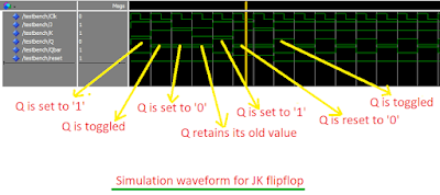
    I want to share the VHDL code for a JK flip flop which is positive edge triggered and has an active high reset input. This flipflop has the following 1 bit inputs: Clock, J, K and reset. The outputs are Q and Qbar. Qbar is always 'not' of Q

    The code is written using behavioral modelling. When the reset is low( '0' ) and the value of Clk changes from 0 to 1, we check the value of J and K through if else statements and set the value of Q and Qbar accordingly. 

    The reset input in this JK flipflop is said to be asynchronous because its value is checked independent of the state of the clock signal.

VHDL Code for JK Flipflop:


--libraries to be used are specified here
library ieee;
use ieee.std_logic_1164.all;

--entity declaration with port definitions
entity JK_flipflop is
port(Clk : in std_logic;  --positive edge triggered
    J, K: in std_logic;
    reset: in std_logic;  --active high reset
    Q, Qbar: out std_logic
    );
end JK_flipflop;

--architecture of entity
architecture Behavioral of JK_flipflop is

--temporary signals.
--they are used because, output ports cannot be read in the VHDL versions prior to 2008.
signal qtemp, qbartemp : std_logic := '0';

begin

--assign the temporary signals to corresponding output ports.
--'Qbar' is always 'not' of 'Q'.
Q <= qtemp;
Qbar <= qbartemp;

--process for JK flip flop
process(Clk,reset)
begin
if(reset = '1') then           --Reset the output when reset is high
    qtemp <= '0';
    qbartemp <= '1';
elsif(rising_edge(clk)) then
    if(J='0' and K='0') then       --No change in the output
        NULL;
    elsif(J='0' and K='1') then    --Set the output Q.
        qtemp <= '0';
        qbartemp <= '1';
    elsif(J='1' and K='0') then    --Reset the output Q.
        qtemp <= '1';
        qbartemp <= '0';
    else                           --Toggle the output Q.
        qtemp <= not qtemp;
        qbartemp <= not qbartemp;
    end if;
end if;
end process;

end Behavioral;

Testbench code for JK Flipflop:


--library declarations
library ieee;
use ieee.std_logic_1164.all;

--this is how entity for your test bench code has to be declared.
entity testbench is
end testbench;

architecture behavior of testbench is

--Signal declarations
signal Clk,J,K,reset,Q,Qbar : std_logic := '0';
-- Clock period definitions
constant Clk_period : time := 10 ns;

begin

-- Instantiate the Unit Under Test (UUT). 
--This style is known as entity instantiation with named association
UUT : entity work.JK_flipflop 
    port map(Clk => Clk,
        J => J,
        K => K,
        reset => reset,
        Q => Q,
        Qbar => Qbar);

--Generate Clk with a period of 'Clk_period'
Clk_generation: process
begin
    Clk <= not Clk;  --toggle 'Clk' when half 'Clk_period' is over.
    wait for Clk_period/2;
end process;

-- Stimulus process
stimulus: process
begin        
    --change J and K and wait for a Clock period to see the changes
    J<='1'; K<='0'; wait for Clk_period;
    J<='1'; K<='1'; wait for Clk_period;
    J<='0'; K<='1'; wait for Clk_period;
    J<='0'; K<='0'; wait for Clk_period;
    J<='1'; K<='0'; wait for Clk_period;
    --apply reset input and change J and K.
    reset <='1';
    J<='1'; K<='1'; wait for Clk_period;
    J<='0'; K<='1'; wait for Clk_period;
    --reset is made 'low' again.
    reset <='0';
    --now onwards, Q will keep toggling between 1 and 0.
    J<='1'; K<='1'; wait for Clk_period;
    wait;
end process;

end;

Simulation Waveform:


The codes were simulated in Modelsim. This is a screenshot of the waveform.

simulation waveform of jk flipflop in vhdl modelsim


    The code was synthesized using Xilinx ISE. The RTL schematic of the design is shown below:

    In the schematic FDPE represents a single D-type flip-flop with data (D), clock enable (CE), and asynchronous preset (PRE) inputs and data output (Q). Similarly FDCE represents a single D-type flip-flop with data (D), clock enable (CE), and asynchronous clear (CLR) inputs and data output (Q). 


rtl schematic of jk flipflop in xilinx ise

Note
 :- Use RTL Viewer to get a closer look on how your design is actually implemented in hardware.

VHDL: 3 to 8 Decoder with Testbench (Gate Level Modelling)

    I want to share the VHDL code for a 3 to 8 decoder implemented using basic logic gates such as AND, OR etc.. The entity port has one 3-bit input and one 8-bit decoded output. 

    Only one bit in the output is high at any given time. And the index of the bit which is high at any given moment is decided by the value of encoded input. Since input is 3 bit, it can have a maximum of 8 (2^3) unique values, which correspond to the size of the output vector. 

Circuit Diagram:


The circuit diagram for the decoder is given below. This diagram is taken from javatpoint. You can also see the truth table from the same website. 

circuit diagram for 3 to 8 decoder


VHDL Code for 3:8 Decoder:


--libraries to be used are specified here
library ieee;
use ieee.std_logic_1164.all;

--entity declaration with port definitions
entity decoder_3to8 is
port(input : in std_logic_vector(2 downto 0);  --3 bit input
     output : out std_logic_vector(7 downto 0)  -- 8 bit decoded output
   );
end decoder_3to8;

architecture gate_level of decoder_3to8 is

begin 

output(0) <= (not input(2)) and (not input(1)) and (not input(0));
output(1) <= (not input(2)) and (not input(1)) and input(0);
output(2) <= (not input(2)) and input(1) and (not input(0));
output(3) <= (not input(2)) and input(1) and input(0);
output(4) <= input(2) and (not input(1)) and (not input(0));
output(5) <= input(2) and (not input(1)) and input(0);
output(6) <= input(2) and input(1) and (not input(0));
output(7) <= input(2) and input(1) and input(0);

end gate_level;

A little tip on Concurrency in VHDL:


    We have used basic logic gates here to implement the decoder. This is known as Gate Level Modelling in VHDL. 
    
    All the statements in the architecture body in the above code are concurrent, which means they execute parallelly. If you feel that the line order matters in the above code you can try changing them. But you would still get the same results in the simulation waveform.

Testbench code for 3:8 Decoder:


--library declarations
library ieee;
use ieee.std_logic_1164.all;

--this is how entity for your test bench code has to be declared.
entity testbench is
end testbench;

architecture behavior of testbench is

--signal declarations.
signal input : std_logic_vector(2 downto 0) := (others => '0');
signal output :  std_logic_vector(7 downto 0) := (others => '0');

begin

--entity instantiation with name association
uut : entity work.decoder_3to8 
    port map(input => input,
        output => output);

--definition of simulation process
stimulus : process 
begin
    --after changing 'input' wait for a bit to see the results in the simulation waveform
    input<="000";  --input = 0.
    wait for 2 ns;
    input<="001";   --input = 1.
    wait for 2 ns;
    input<="010";   --input = 2.
    wait for 2 ns;
    input<="011";   --input = 3.
    wait for 2 ns;
    input<="100";   --input = 4.
    wait for 2 ns;
    input<="101";   --input = 5.
    wait for 2 ns;
    input<="110";   --input = 6.
    wait for 2 ns;
    input<="111";   --input = 7.
    wait;  --wait indefinitely. simulation over.
end process stimulus;

end;

Simulation Waveform:


The codes were simulated in Modelsim. This is a screenshot of the waveform.

simulation waveform of 3:8 decoder in vhdl using modelsim

RTL Schematic:


The code was synthesized using Xilinx ISE . The RTL schematic of the design is shown below:


rtl schematic of 3:8 decoder

Note :- Use RTL Viewer to get a closer look on how your design is actually implemented in hardware.


Fixed Point Operations in VHDL : Tutorial Series Part 1

     You must have heard about library named fixed_pkg.In terms of complexity this library can be placed some where between integer math and floating point maths.I have decided to write a series of tutorials about the usage of fixed_pkg library.The library helps to handle fractional numbers with ease.
The library can be downloaded from here.

In the first part of this tutorial, I will give an introduction about the library and the new data types available for use.

How to use this library in your module?
Add the following two lines to your code(the place where you usually add the libraries):

library ieee_proposed;
use ieee_proposed.fixed_pkg.all;

What are the new data types available in the package?
     FIXED_PKG defines two new data types.They are UFIXED ( for unsigned fixed point) and SFIXED (for signed fixed point).

How to declare signals?
Say you want a fixed point unsigned signal with 'a' bits for decimal part and 'b' bits for fractional part,then you can declare them as follows:

signal example : ufixed( a-1 downto -b);
--an example
signal example : ufixed (3 downto -4);

Here the signal 'example' has 4 bits for decimal part and 4 bits for fractional part.
example = 9.75 = "1001.1100" or simply example ="10011100".

For signed numbers we use "sfixed" while declaring the signals.Signed numbers are stored as 2's complement format.


--an example for signed fixed point type.
signal example : sfixed(4 downto -4);

     Here the signal 'example' has 5 bits of decimal part and 4 bits for fractional part.
example = -9.75 = "101100100".This is got by taking 2's complement of binary value of 9.75.The MSB bit '1' indicates the number as negative.

If you declare the signal as sfixed and still store a positive value(say 9.75) then it has the same kind of storage format as ufixed.


--an example
signal example : sfixed(4 downto -4);
--If 'example' contains 9.75 then it is storage as "01001.1100".

     Remember that you declare the signals with sufficient width so that values are get stored correctly.If the width is not enough then the signal may get rounded off.

VHDL: 4 bit Ripple Carry Adder with Testbench (Gate Level Modelling)

    I want to share the VHDL code for a 4-bit Ripple carry adder(RCA) implemented using basic logic gates such as AND, OR, XOR etc.. The entity port has two 4-bit inputs and one 1-bit carry input. There are two outputs, a 4-bit sum and a 1-bit carry.

    Why is this adder called ripple carry? If you look at the block diagram below, the respective bits from the input operands are fed to the full adders. And then the carry out from each full adder is fed as the carry in of the next full adder. In a way you can say that the carry is rippled from the right(least significant bit position) to the left(most significant bit position) side. 


VHDL Code for 4 bit Ripple Carry Adder:


--libraries to be used are specified here
library ieee;
use ieee.std_logic_1164.all;
use ieee.numeric_std.all;

--entity declaration with port definitions
entity rc_adder is --ripple carry adder
port(num1 : in unsigned(3 downto 0);  --4 bit input 1
    num2 : in unsigned(3 downto 0);   --4 bit input 2
    sum : out unsigned(3 downto 0);   --4 bit sum
    carry : out std_logic                     -- carry out.
);
end rc_adder;

--architecture of entity
architecture gate_level of rc_adder is

--temporary signal declarations(for intermediate carry's).
signal c0,c1,c2,c3 : std_logic := '0';

begin  

--first full adder
sum(0) <= num1(0) xor num2(0);  --sum calculation
c0 <= num1(0) and num2(0);      --carry calculation
--second full adder
sum(1) <= num1(1) xor num2(1) xor c0;
c1 <= (num1(1) and num2(1)) or (num1(1) and c0) or (num2(1) and c0);
--third full adder
sum(2) <= num1(2) xor num2(2) xor c1;
c2 <= (num1(2) and num2(2)) or (num1(2) and c1) or (num2(2) and c1);
--fourth(final) full adder
sum(3) <= num1(3) xor num2(3) xor c2;
c3 <= (num1(3) and num2(3)) or (num1(3) and c2) or (num2(3) and c2);
--final carry assignment
carry <= c3;

end gate_level;

A little tip on Concurrency in VHDL:


    We have used basic logic gates here to implement the adder. This is known as Gate Level Modelling in VHDL. 
    
    All the statements in the architecture body in the above code are concurrent, which means they execute parallelly. But since the output of one gate is connected as the input to another, they appear as concatenated and looks as if the first line executes first before the second line. 

    If you are not convinced of what I am saying, you can change the line order as you like, and you would still get the same simulation waveform.

Testbench code for Ripple carry adder:


--library declarations
library ieee;
use ieee.std_logic_1164.all;
use ieee.numeric_std.all;

--this is how entity for your testbench code has to be declared.
entity testbench is
end testbench;

architecture behavior of testbench is

--signal declarations.
signal num1,num2,sum : unsigned(3 downto 0) :=(others => '0');
signal carry :  std_logic:='0';

begin

--entity instantiation
adder : entity work.rc_adder 
    port map(num1 => num1,
        num2 => num2,
        sum => sum,
        carry => carry);

--definition of simulation process
stimulus : process
begin
    --result should be sum=11 and carry=0
    num1 <= to_unsigned(2,4);  
    num2 <= to_unsigned(9,4);  
    wait for 2 ns; 

    --result should be sum=13 and carry=0
    num1 <= to_unsigned(10,4);  
    num2 <= to_unsigned(3,4);  
    wait for 2 ns;

    --result should be sum=14 and carry=0
    num1 <= to_unsigned(8,4);  
    num2 <= to_unsigned(6,4);  
    wait for 2 ns;

    --result should be sum=0 and carry=1
    num1 <= to_unsigned(10,4);  
    num2 <= to_unsigned(6,4);  
    --more input combinations can be given here.
    wait;
end process stimulus;

end;

Simulation Waveform:


The codes were simulated in Modelsim. This is a screenshot of the waveform.

simulation waveform of 4 bit ripple carry adder in vhdl modelsim

RTL Schematic:


The code was synthesized using Xilinx ISE . The RTL schematic of the design is shown below:


rtl schematic of 4 bit ripple carry adder in xilinx ise

Note :- Use RTL Viewer to get a closer look on how your design is actually implemented in hardware.